- Longgang District, Shenzhen City
- Mon - Sat 8:00 - 6:30
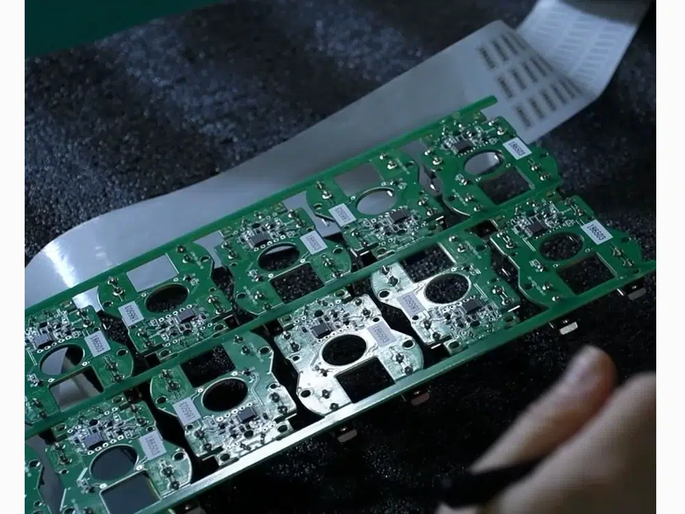
What is HDI PCB?
An HDI PCB (High-Density Interconnect Printed Circuit Board) is a type of circuit board that packs more wiring density per unit area than conventional PCBs. According to IPC-2226, the international standard for HDI design, these boards are characterized by:
- Finer lines and spaces (≤100 µm or 0.10mm)
- Smaller vias with diameters less than 150 µm
- Capture pads smaller than 400 µm (0.40mm)
- Higher connection pad density (more than 20 pads per cm²)
What makes HDI PCB technology special is its use of microvias—laser-drilled holes typically ranging from 50 to 150 microns in diameter. These tiny vias, combined with blind and buried via structures, allow designers to create compact, high-performance boards that would be impossible with traditional through-hole technology.
Why HDI PCB Matters in Modern Electronics
The push toward smaller devices with more functionality has made HDI PCB technology essential. Your smartphone, for instance, contains a motherboard that would have filled an entire desktop computer just 20 years ago. This miniaturization is possible because HDI PCB technology allows:
- Higher component density: More components fit in smaller spaces
- Better signal integrity: Shorter signal paths reduce delays and crosstalk
- Reduced layer count: An 8-layer conventional board can often become a 4-layer HDI board
- Lighter weight: Critical for portable and wearable devices
- Improved reliability: Smaller aspect ratios in microvias mean better plating and fewer failures
The global HDI PCB market was valued at approximately $16.2 billion in 2024 and is projected to reach $24.8 billion by 2029, according to industry research. This growth reflects just how fundamental HDI technology has become across consumer electronics, automotive, medical devices, and telecommunications.
we partner with leading companies in numerous markets to deliver solutions for their most complex challenges.
Contact
- 6th Floor, Building A, Yiyuantong Industrial Park, No. 22, Zhonghao 2nd Road, Bantian Sub-district, Longgang District, Shenzhen City
- © Copyright 2025 by www.strongki.cn/