- Longgang District, Shenzhen City
- Mon - Sat 8:00 - 6:30
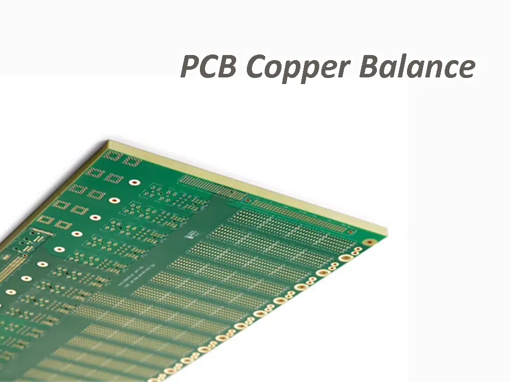
PCB Fabrication
Once the design is verified, the next step is PCB fabrication. This process involves creating the bare PCB that will serve as the foundation for component assembly.
-
Material Selection: The process begins by selecting the appropriate base material, typically a form of fiberglass with copper layers.
-
Imaging: The PCB design is transferred onto the copper layers using photolithography techniques.
-
Etching: Excess copper is removed, leaving only the desired circuit patterns.
-
Drilling: Holes are drilled for through-hole components and vias.
-
Plating: The board is plated with additional copper to ensure good connectivity.
-
Solder Mask and Silkscreen: A solder mask is applied to protect the copper traces, and a silkscreen is added for component labels and other markings.
The result of this step is a bare PCB ready for component assembly.
6 Tips for Choosing Components for Your PCBA
Selecting the right components is crucial for the success of your PCB assembly project. Here are six important tips to consider:
1. Procure Components from a Reliable Supplier
- Choose suppliers with a good reputation for quality and reliability.
- Ensure the supplier can provide authentication and traceability for components.
- Consider suppliers who offer component lifecycle management services.
2. Opt for IC Packages to Reduce the Part Count
- Integrated Circuits (ICs) can often replace multiple discrete components.
- Reducing part count can lower assembly costs and improve reliability.
- However, balance this with considerations for repair and component availability.
3. Select SMT Components as Much as Possible
- SMT components are generally smaller and allow for higher density designs.
- They are well-suited for automated assembly, which can reduce costs and improve consistency.
- SMT components often have better high-frequency performance than through-hole equivalents.
4. Consider Component Footprint
- Choose components with footprints that match your PCB design constraints.
- Smaller footprints allow for more compact designs but may increase assembly complexity.
- Ensure your assembly partner has the capability to handle the chosen component sizes.
5. Consider Cost and Availability
- Balance component performance with cost considerations.
- Check the availability of components to avoid supply chain issues.
- Consider alternative or pin-compatible components for critical parts to mitigate supply risks.
6. Managing Component Delivery
- Plan component delivery to align with your production schedule.
- Consider just-in-time delivery for high-volume production to reduce inventory costs.
- For critical or long-lead-time components, consider maintaining a safety stock.
we partner with leading companies in numerous markets to deliver solutions for their most complex challenges.
Contact
- 6th Floor, Building A, Yiyuantong Industrial Park, No. 22, Zhonghao 2nd Road, Bantian Sub-district, Longgang District, Shenzhen City
- © Copyright 2025 by www.strongki.cn/